

| Optical Loss | Max. Bandwidth | Half-Wave Voltage Vπ | Extinction Ratio | Chip Length | Linearity | Integration | Cost | |
|---|---|---|---|---|---|---|---|---|
| LiNbO3 | ||||||||
| InP | ||||||||
| SiPh | ||||||||
| TFLN | Excellent | Excellent | Excellent | Excellent | Medium | Excellent | Medium | Medium |
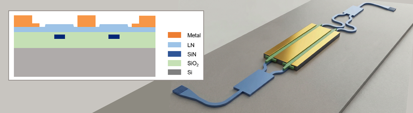
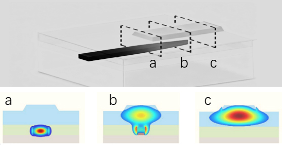
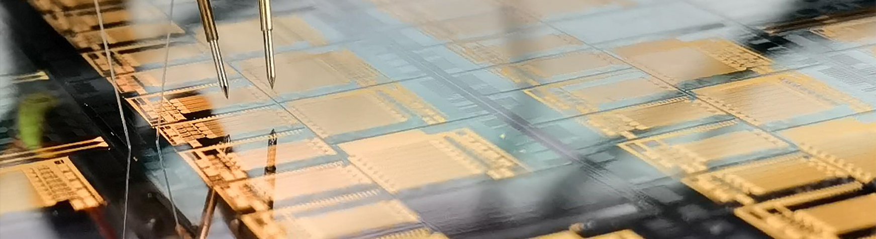
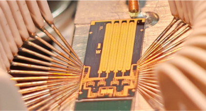
Low-Loss vertical inter-waveguide coupling
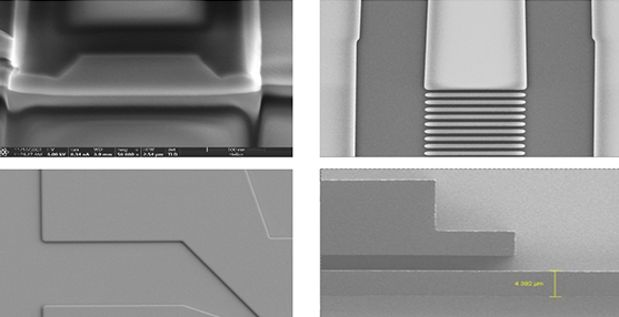
Lithium niobate and electrode processing specialized for 4"/6" heterogenous wafers
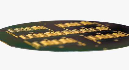
Wafer dicing and polishing specialized for 4"/6" heterogenous wafers
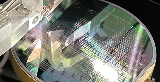
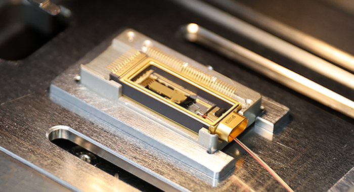
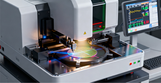
Wafer and chip testing specialised for 4''/6'' heterogenous wafers